DEK: Mass Imaging Process
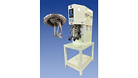
DEK has successfully applied mass imaging techniques to improve the uniformity of Thermal Interface Material deposited between a silicon die and its package lid during semiconductor packaging processes. By mass imaging the TIM using ProFlow DirEKt Imaging, semiconductor manufacturers can now be sure that the die surface is covered by a uniform thickness of TIM. Advantages include better thermal connectivity between the die and the lid, which improves reliability as well as greater coplanarity of the lid. The company will also soon conclude development of a lid-sealing process that will complement its TIM deposit process to create a complete mass imaging solution for lid attachment.
For more information, call 908-782-4140 or fax 908-782-4774.
Looking for a reprint of this article?
From high-res PDFs to custom plaques, order your copy today!


