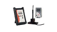
The 3D-IC automated metrology system provides imaging technology to verify the alignment of bonded wafers and through silicon vias (TSVs). The 3-D interconnect process using TSVs requires bonding the active side of processed wafers together. The accuracy of the bonding alignment needs to be immediately verified once the wafers are bonded, but the active wafer surfaces containing the alignment targets are no longer visible; the metrology system allows observation and image acquisition by "seeing" through up to 1200 µm of bulk silicon to the patterned surfaces.
For more information, phone (408) 514-3900 or visitwww.olympus-ita.com.
OLYMPUS INTEGRATED TECHNOLOGIES AMERICA: Metrology System
Looking for a reprint of this article?
From high-res PDFs to custom plaques, order your copy today!


